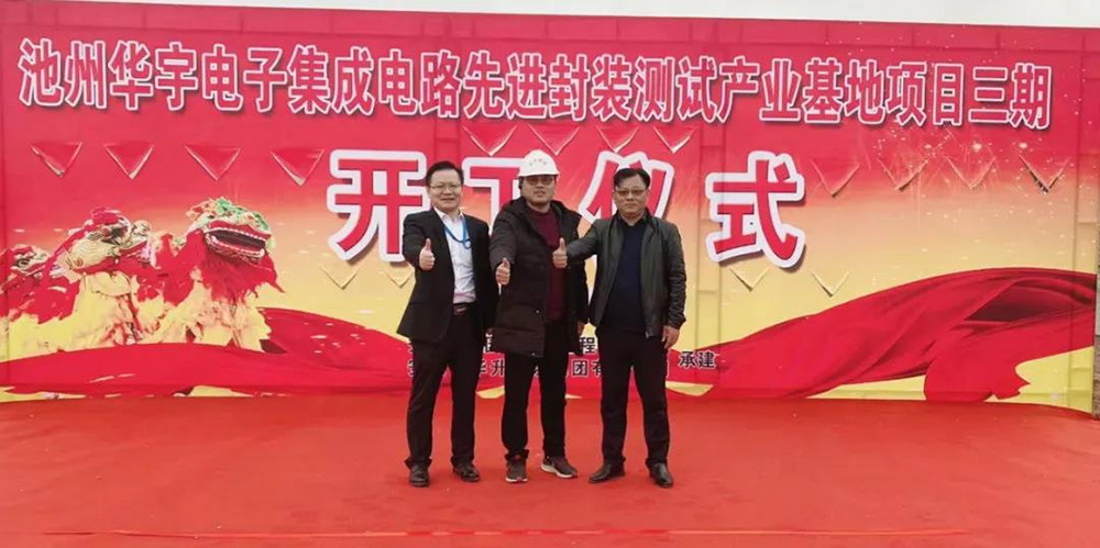
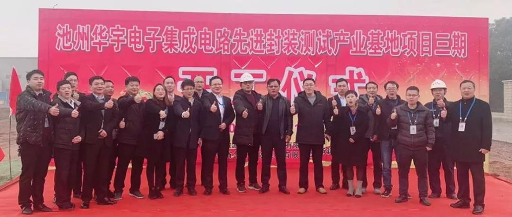
At 9:28 on The morning of December 15, Chizhou HISEMI Electronic Technology Co., LTD. Phase III project was held.

The total investment of the third phase project is 1 billion yuan, with a total construction area of 45,000 square meters. After the project reaches the stage, the annual sales will reach 2.5 billion yuan, making the company step into the ranks of advanced packaging in a real sense. The packaging technology will upgrade to SIP system-level 3D packaging technology, LGA and BGA advanced packaging technology, and it is expected to be put into production in 2022.

In the future, the company will develop into a world-renowned semiconductor packaging and testing enterprise, continue to innovate, and strive to make Hisemi Electronics leap into the world’s top 10 semiconductor packaging and testing industry, holding the enterprise mission of “Huayu Xin, the dream of a powerful country”. Congratulations on the successful commencement ceremony of the third phase of the company’s project, and wish the company a successful completion of the third phase of the project!


